Ice Plume Particle Detector
A charged ice particle detection instrument for a spacecraft flying through Enceladus' ice ejecta plumes
Project Overview
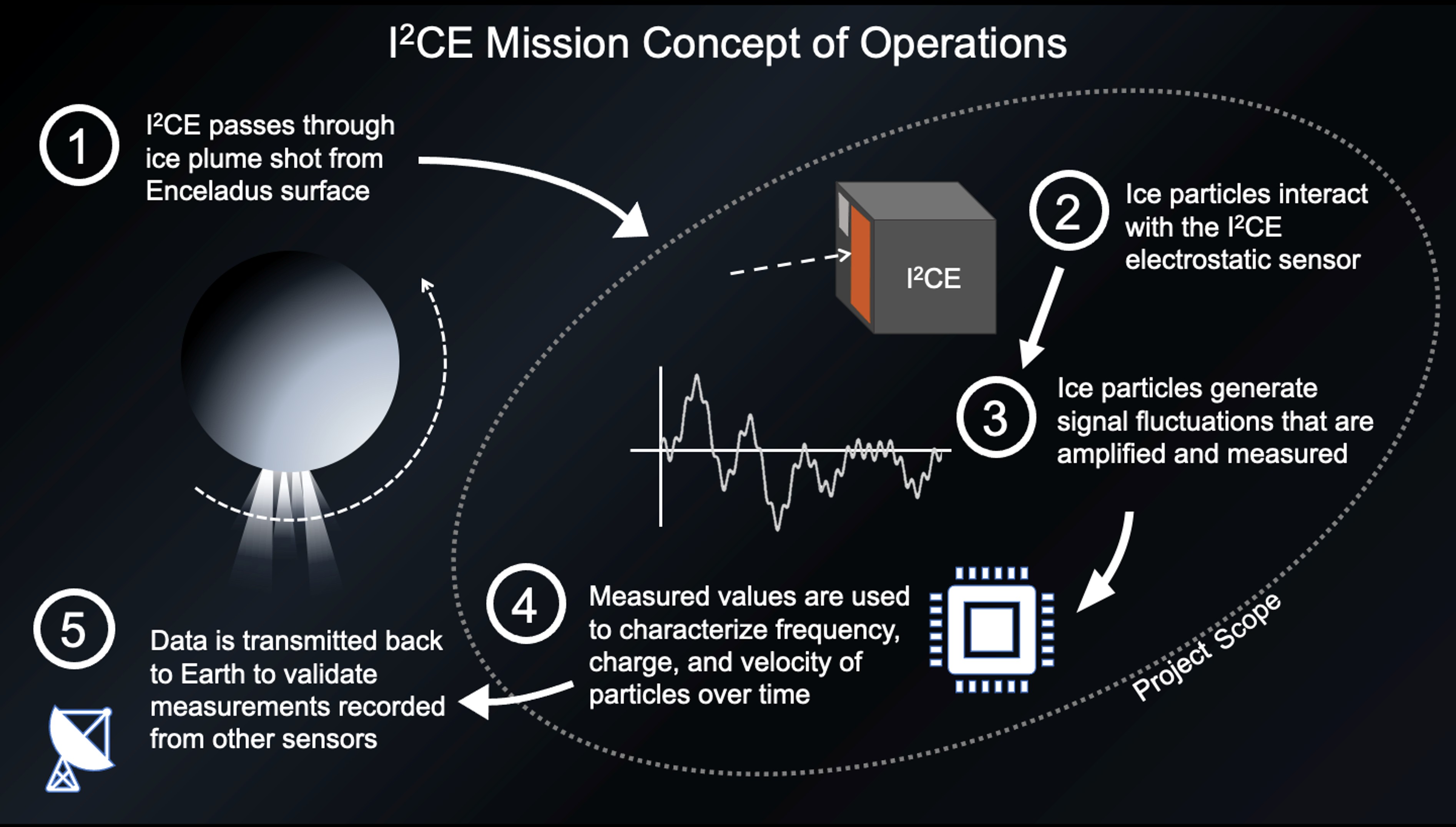
Mission
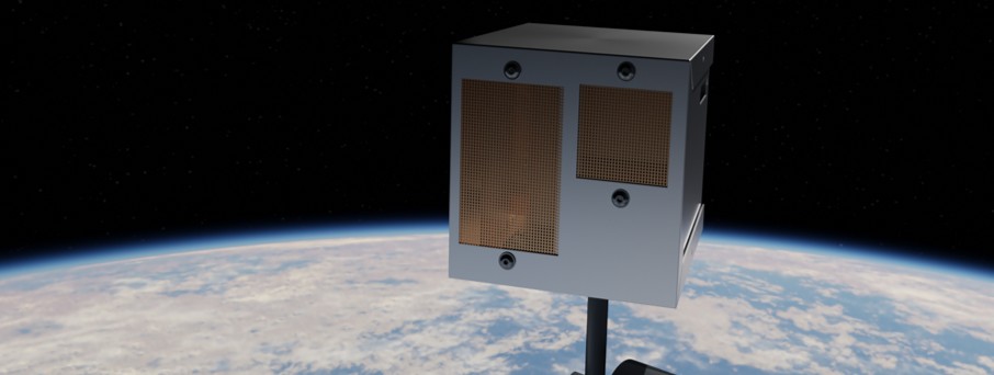
This project focused on developing and prototyping a charged particle detection instrument designed for spacecraft flying through Enceladus' ice plumes. Geysers on the south pole of Saturn's moon eject water into space, where a satellite sent by the project's sponsor, ASTROBi, would pass through it. This detector would enable in-situ analysis of the relative magnitude of ice particles that the satellite is passing through.
Challenge
Design a proof-of-concept sensor that can reliably detect when a spacecraft is inside Enceladus’ ice plumes and characterize individual, weakly charged micron-scale particles (0.5–4 µm; 100–300 m/s) by their presence, charge, and speed. The system must operate in a vacuum, and fit within a 1U (10cm x 10cm x 10cm) and operate at < 10 Watts.
Solution
Constructed a dual-mode electrostatic charge detector that combines a conduction-based cup (bulk charge flux) with a grid-based induction stage (individual particle charge and speed), using custom charge amplifiers, a 1 Million samples per second (MSPS) ADC, and a convolution filter event detection system on a Raspberry Pi. My main role involved the development of the sensor electronics and software integration.
Technologies & Tools
Design & Development
Electronics Design
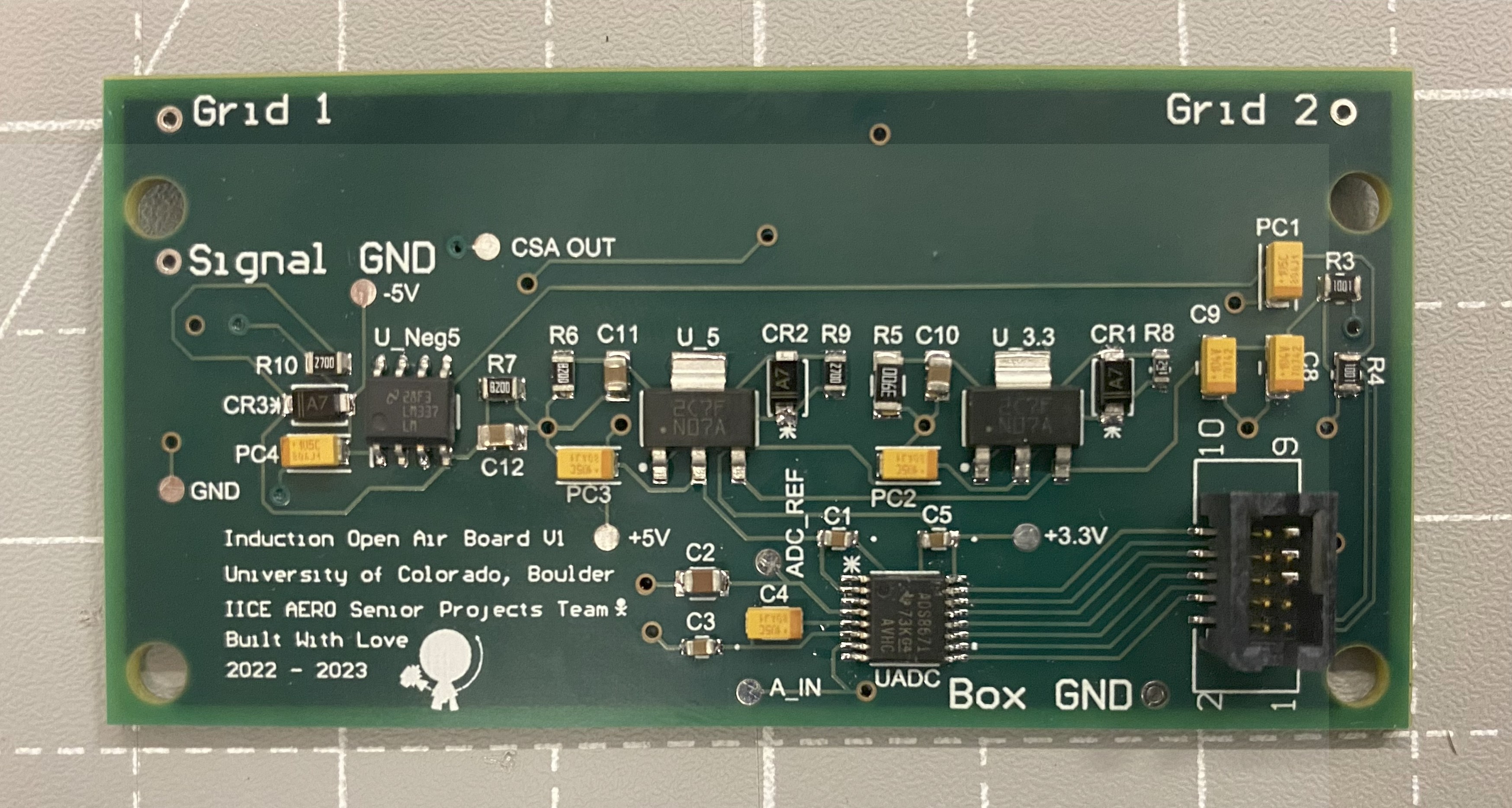
Designed a custom PCB layouts for sensor signal conditioning, amplification, and digitization. Implemented low-noise circuitry to handle extremely small charge signals (~300 electrons) from individual particle impacts.
- Custom charge amplifier circuits with sub-pA noise floors
- Multi-channel data acquisition system
- EMI/EMC protected system for noise reduction
- Surface mount PCB development
Mechanical Systems
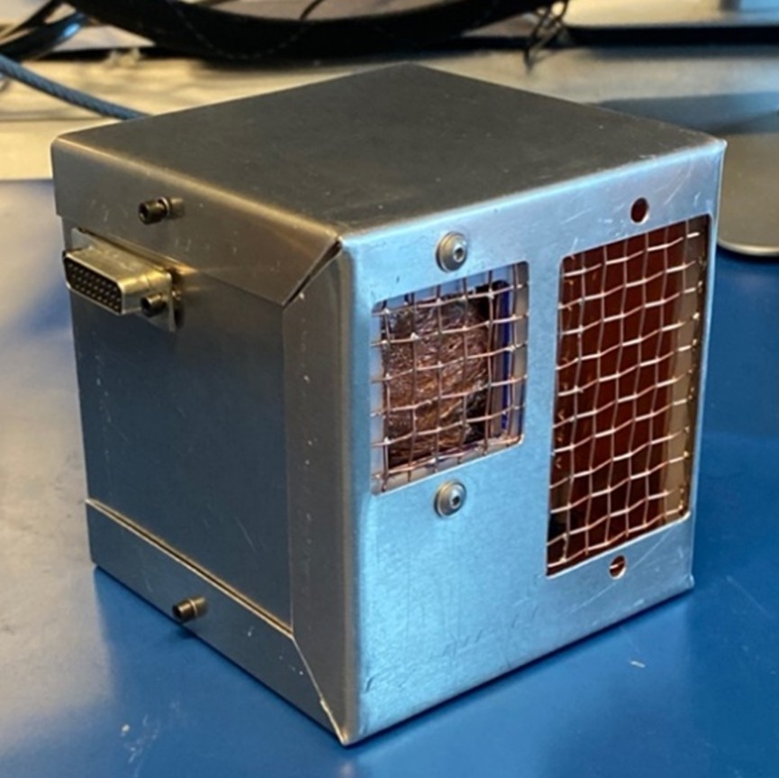
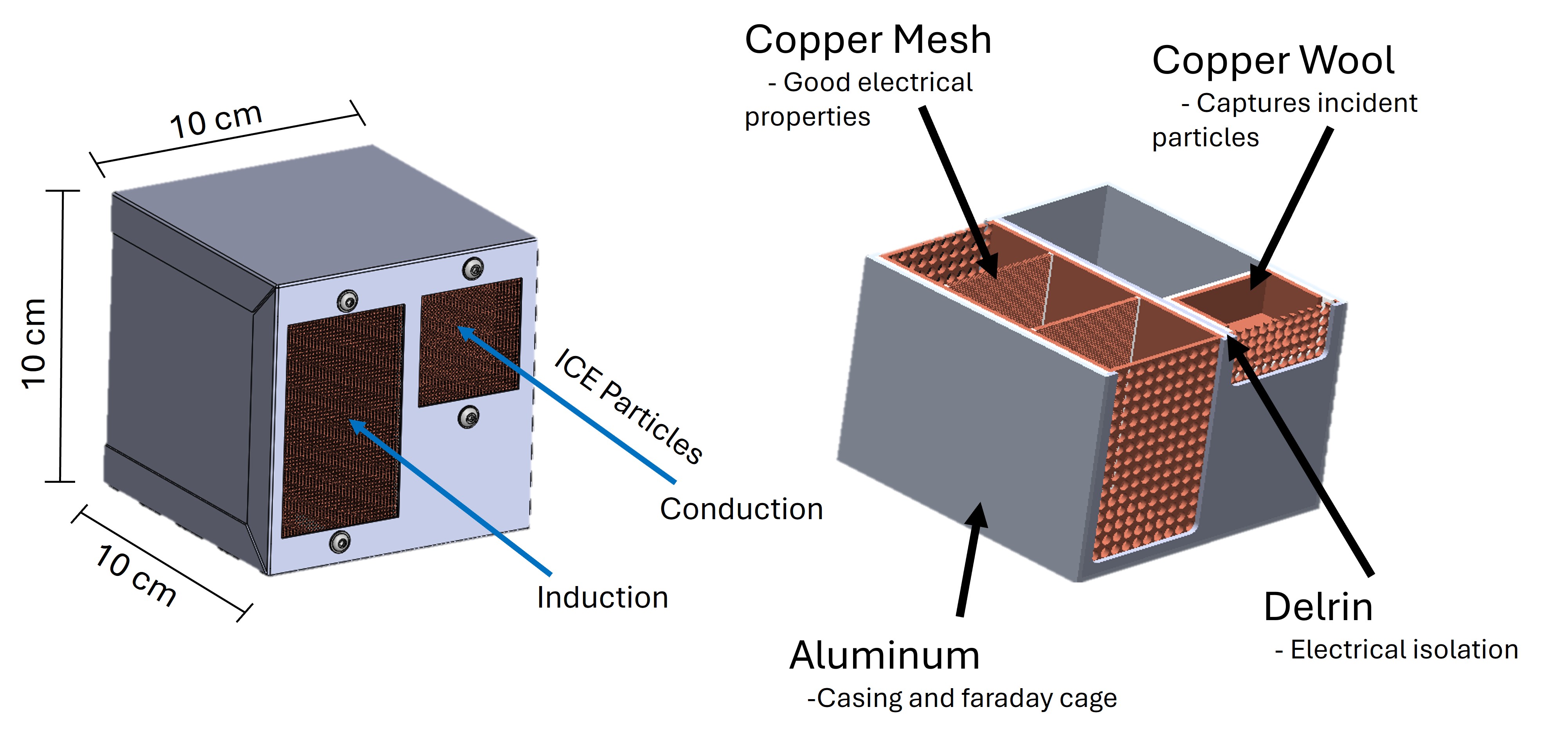
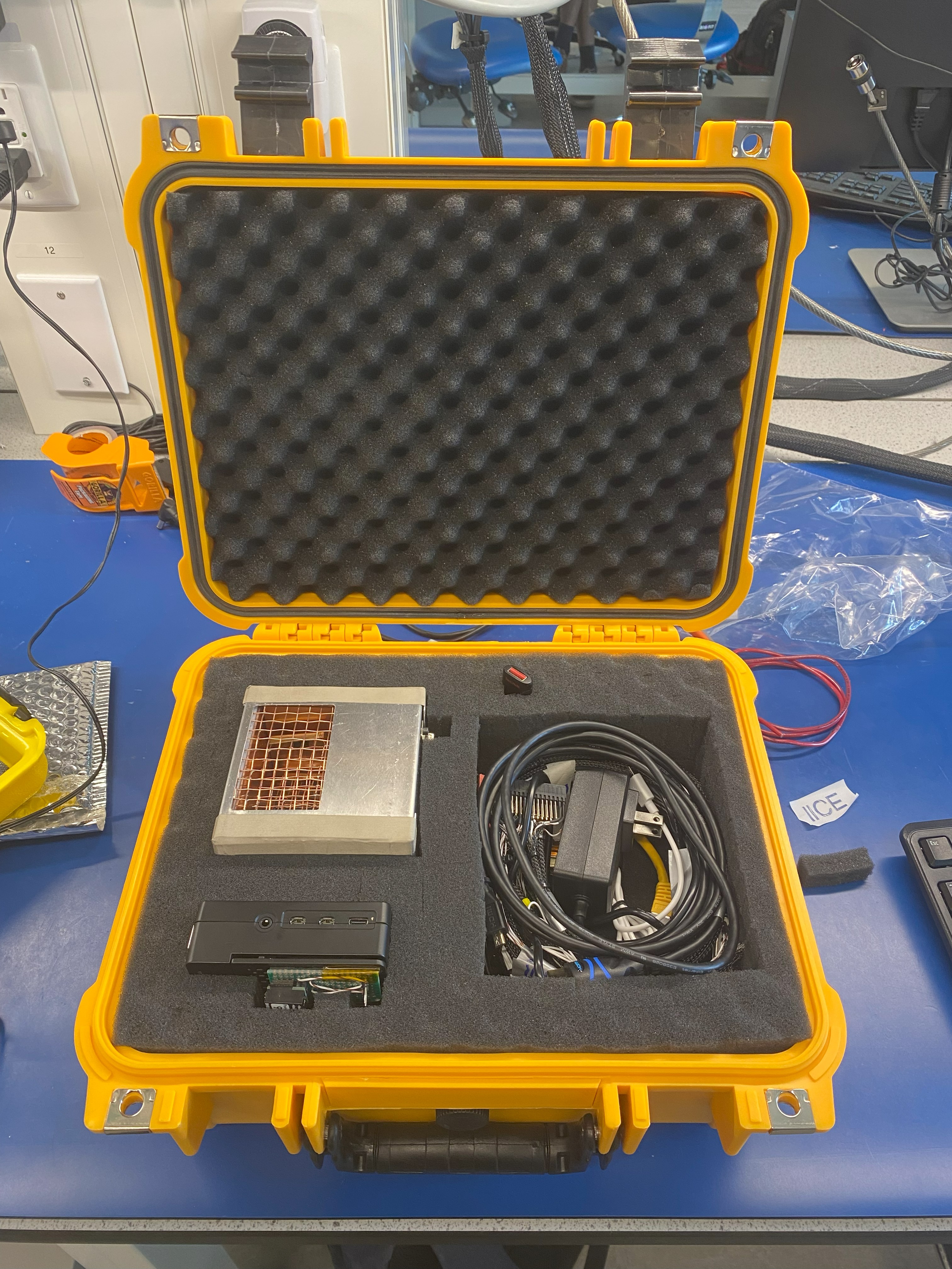
Developed mechanical housing and sensor structures using SolidWorks. Ensured structural integrity for shipping and handling while maintaining required faraday cage capabilities, electrical noise isolation, and thermal dissipation requirements.
- CAD modeling and FEA structural analysis
- Thermal management and insulation design
- EMI/EMC noise analysis and optimization
- Management of extremely tight packaging restrictions
Software & Data Processing
Implemented real-time data acquisition and processing algorithms in C++ and Python. Developed MATLAB analysis tools for post-processing and scientific interpretation of particle measurements.
- Real-time signal processing algorithms to handle 1 million voltage samples collected per second
- Automated particle event detection and classification
- Data compression for efficient storage
- Ground support equipment & testing software
Technical Specifications
Power Requirements
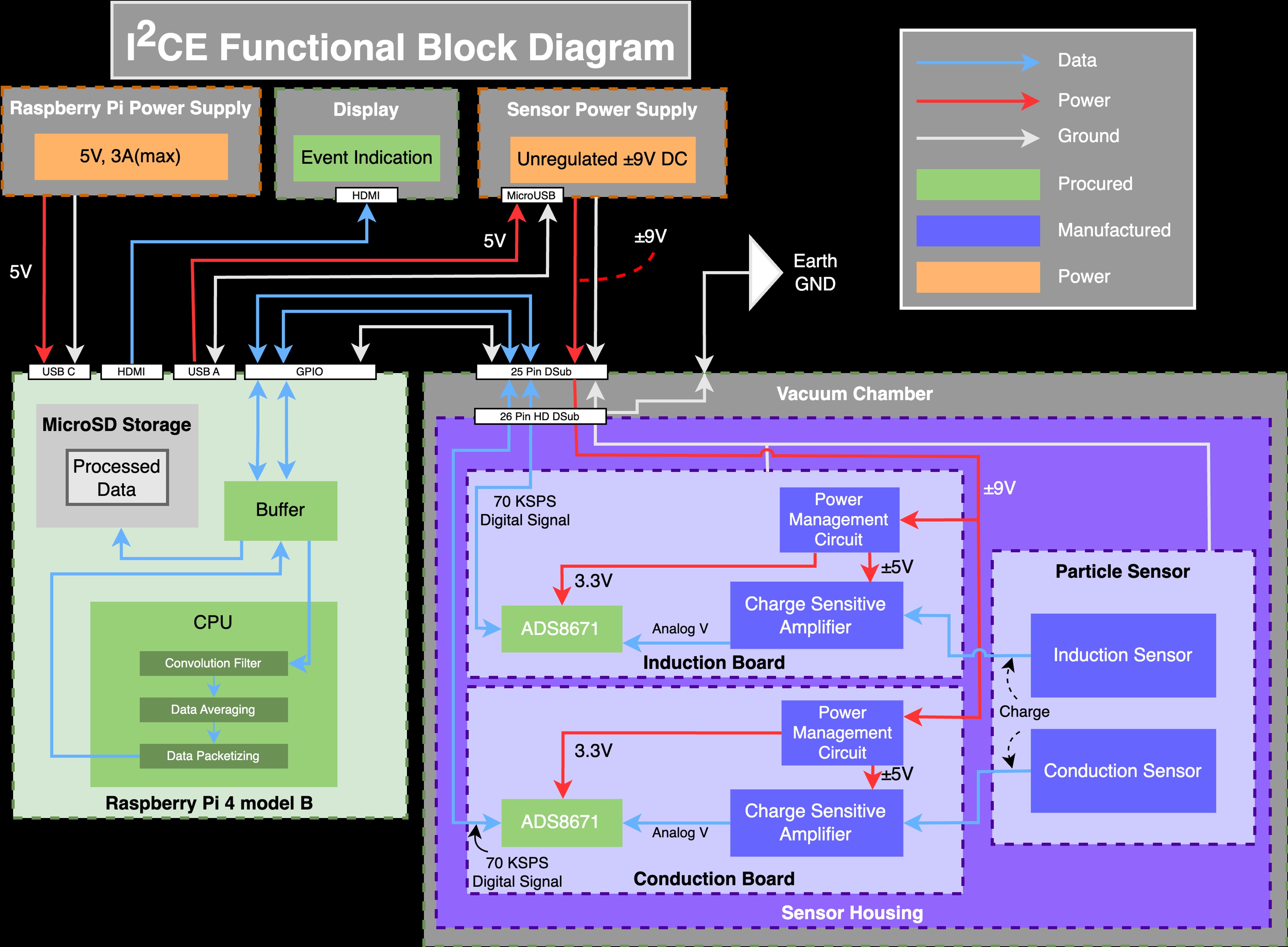
Input Rails: ±9 V to sensor; locally regulated to +3.3 V (ADC) and ±5 V (CSAs)
Power Budget: ≤ 10 W (project requirement)
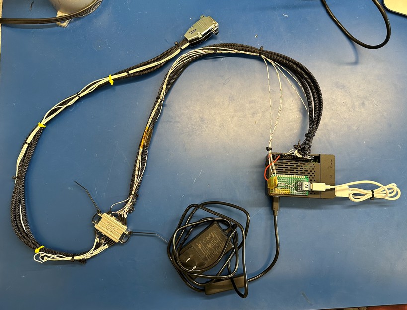
Interface: SPI ADC → Raspberry Pi 4 (1 MSPS per channel) through 25 pin D-Sub
Environmental
Vacuum Compatibility: Operated nominally after survivability test at ~3.82 torr (509 Pa; ~0.005 atm)
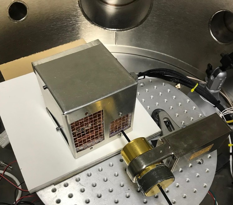
Heat Dissipation: Verified in vacuum (no convection) under load
EMI/Noise Control: Faraday cage enclosure; low-noise analog layout & filtering
Physical Dimensions
Envelope: ≤ 100 mm × 100 mm × 100 mm (CubeSat-class volume constraint)
Mass: TBD
Materials: Aluminum enclosure with copper grids & copper wool internals
Performance
Particle Size (target): 0.5–4 µm
Speed (measured): 100–300 m/s via dual sensing grids
Charge Sensitivity (induction): ~0.05–0.5 fC per particle (3000 extra electrons)
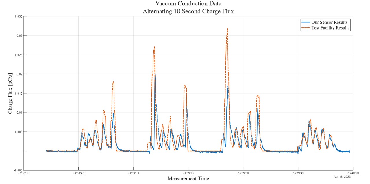
Charge Flux (conduction): Tracked vs reference; design environment ~86 pC/s (500 M electrons/sec)
Sampling: 1 MSPS ADC; convolution-filter event detection
System Architecture
Results & Impact
Key Achievements
Personally Received Award for Technical Knowledge
Was publicly recognized at graduation for exceptional technical knowledge throughout the year for my work on this project. Was 1 of only 2 recipients who received this award.
Prototype Validation Across Four Tests
Completed direct-charge injection, open-air particle, vacuum survivability, and vacuum ice-grain tests with exceptional performance.
Conduction Performance & Calibration
Generated calibration curve with 0.54% average error. In vacuum, sensor's measured charge flux matched test facility’s alternating 10 s pulses and intra-pulse structure with ~0.4 pC/s mean difference (Highly accurate).
Induction Speed Measurement (Open Air)
Dual-grid induction signals yielded velocity estimates within ~4–10% of kinematic expectations across test heights.
Noise Mitigation & Data Pipeline
Faraday-cage enclosure, low-noise CSA design, and 1 MSPS SPI ADC with matched-filter event detection on Raspberry Pi reduced noise and data volume while preserving events.
Requirement Verification
Verified particle presence detection, speed estimation in induction (open air), vacuum compatibility/heat dissipation, and charge-flux tracking in conduction; documented test procedures and results.
Lessons Learned
Up-front requirements flow-down and risk tracking are critical; inventory and change control should live in a single source of truth. Noise was lower than anticipated, so combining induction and conduction electronics (shared power and a dual-channel ADC) could reduce size/cost/complexity. Robust harnessing, power-on indicators, and careful solder/reflow practices are essential; particularly for vacuum-rated components and to prevent trace damage.
Future Work
Focus on generating a calibration curve specific to the vacuum-tested sensor to improve accuracy, redesigning and hardening the induction PCB to prevent solder and trace failures, and consolidating the conduction and induction electronics into a single board using a dual-channel ADC to reduce mass and complexity. Additional goals include integrating automated plume-detection thresholds and real-time plotting directly on the Raspberry Pi, improved wire management for mechanical stability, and conducting more detailed thermal modeling (e.g., via Thermal Desktop) to evaluate performance under expected temperature cycling and material expansion in flight-like environments.
Project Gallery
Let's Connect
I'd be happy to discuss my experience in more detail or explore potential career opportunities.